Prototype to batch SMT, Through-Hole (THT), and mixed-technology assembly with rigorous optical joint inspection, controlled reflow profiling, and direct WhatsApp engineering consultation.
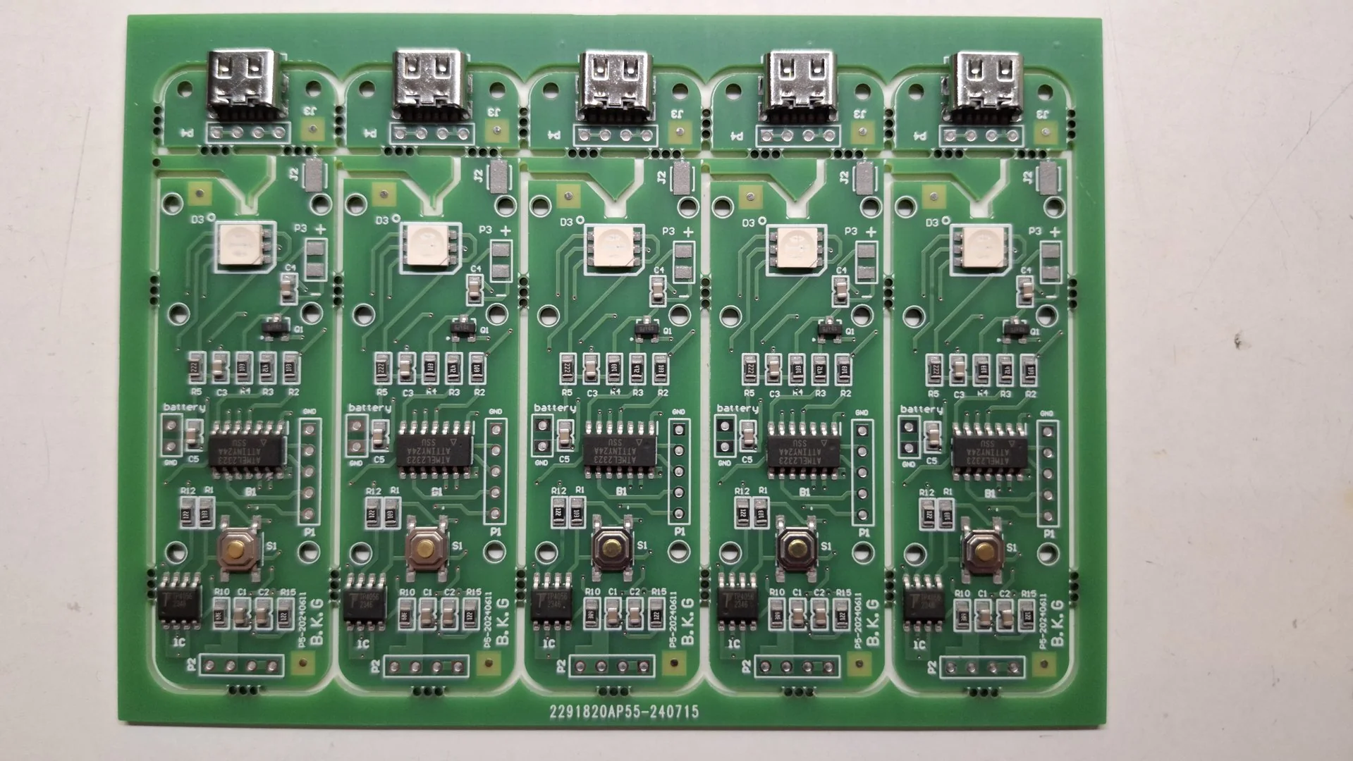
Full-spectrum manufacturing capabilities tailored for hardware engineers, IoT innovators, and industrial equipment builders.
Precision placement of miniature passive parts (0402, 0603, 0805) and multi-pin fine-pitch packages (QFP, QFN, DFN) utilizing stencil paste deposition and reflow soldering.
Clean, high-durability soldering of industrial connectors, terminal blocks, electrolytic capacitors, transformers, and power relays with 100% barrel fill.
Seamless workflow execution for high-density double-sided boards combining bottom/top layer SMD components with bulky through-hole power components.
Detailed microscopic and optical examination of assembled boards to eliminate cold solder joints, unintended bridges, tombstoning, and component misorientation.
Real manufacturing stages from stencil paste printing to controlled reflow and post-assembly quality verification.

Precision fixture clamping and uniform paste rolling across laser stencils ensuring consistent solder volume on every SMD footprint pad.

Organized lead insertion with strict mechanical clearances and reliable through-hole soldering with high-purity solder alloys.

Gentle thermal ramp-up and calibrated soak times preventing thermal shock and producing bright, void-free solder fillets.

Thorough solvent flux cleaning for high-frequency circuits and magnified optical inspection ensuring defect-free shipments.
Actual production boards manufactured and assembled at Crystal Electronics across industrial control, power supplies, IoT, and embedded electronics.
Direct, friction-free collaboration from file sharing to final delivery of assembled boards.
Send your Gerber RS-274X files along with the Bill of Materials (BOM) directly via WhatsApp for swift technical review.
We review component footprints, volume, and turnaround requirements, providing a transparent quotation and lead time.
Laser stencil paste printing, component placement, reflow soldering, through-hole manual work, and chemical cleaning.
100% optical inspection of solder joints, packaging in anti-static ESD shielding bags, and prompt delivery.
At Crystal Electronics, our mission is to deliver dependable soldering quality, precise component placement, and personal engineering responsiveness to electronics developers and manufacturers.
From research prototypes and startup hardware MVPs to batch runs of industrial control boards, every assembly order is executed under ESD-safe procedures with meticulous visual solder verification to guarantee reliable field performance.
Direct communication with the assembly technician with immediate Gerber file review.
Bright, void-free solder joints and thorough flux removal without board discoloration.

Send your board design files and BOM directly on WhatsApp for an immediate feasibility check and quote.
Chat on WhatsApp (+98 912 560 7535)