Specialized PCB Assembly Workshop

Precision Surface Mount & Through-Hole PCB Assembly

Professional manufacturing of SMT, Through-Hole (THT), and mixed-technology printed circuit boards from rapid R&D prototypes to medium-batch production with strict quality control.
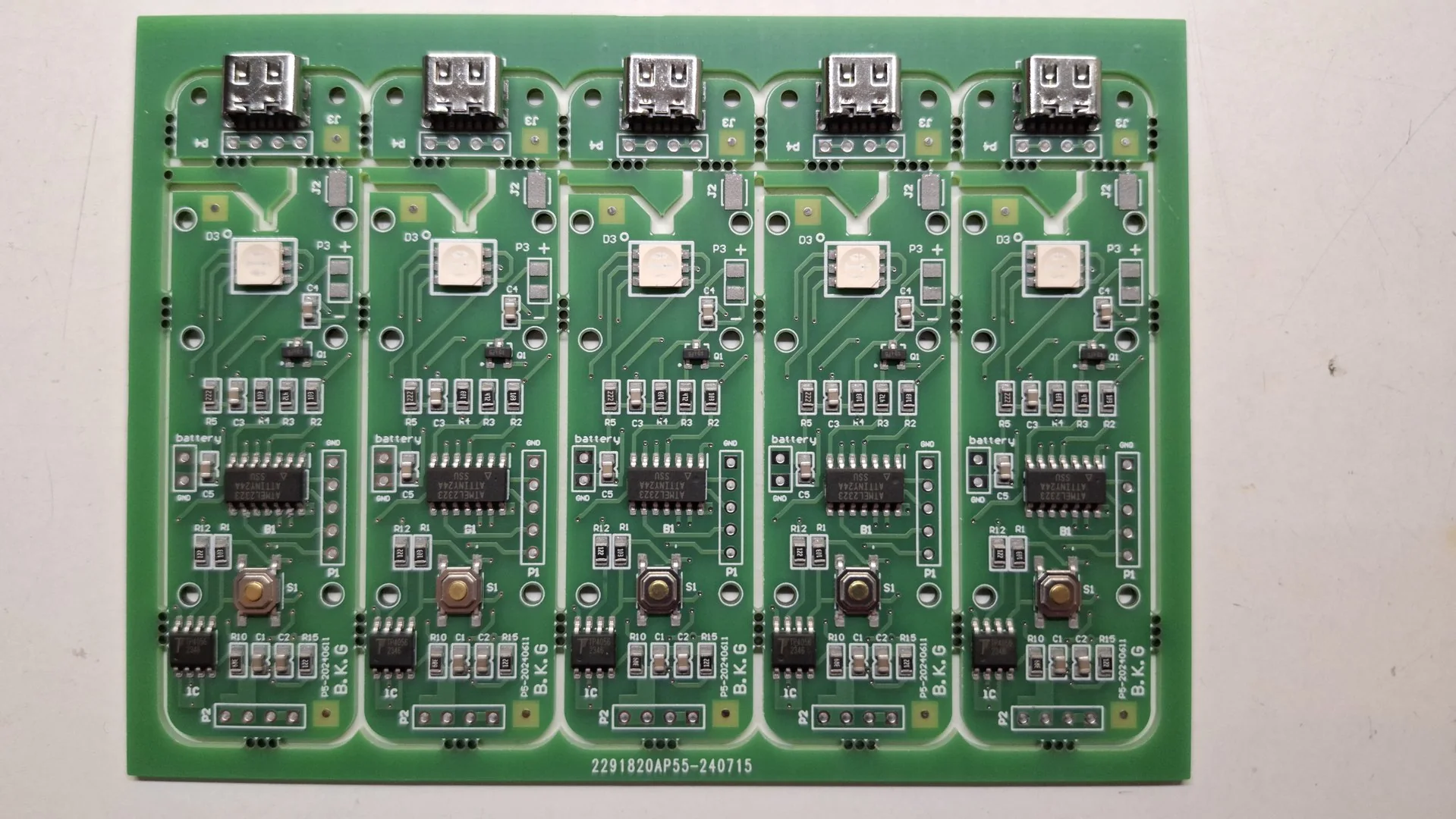
Production line specifications subject to workshop documentation updates
ESD-Protected Workshop
SMT & THT Assembly
Rapid Prototype Turnaround
Crystal Electronics precision solder joint quality
Visual Optical Inspection & Thermal Profiling
INSPECTION ACTIVE
Assembly Capabilities

Specialized PCB Assembly Services

Full-spectrum manufacturing capabilities tailored for hardware engineers, IoT innovators, and industrial equipment builders.

Notice: Detailed line specifications will be updated upon receiving additional workshop documentation

Surface Mount Technology (SMT)

Precision placement of miniature passive parts (0402, 0603, 0805) and multi-pin fine-pitch packages (QFP, QFN, DFN, SOIC) utilizing stencil paste deposition and multi-zone reflow soldering.

  • Laser-cut stainless stencil solder paste application
  • Accurate fine-pitch multi-pin placement
  • Controlled reflow thermal zone profiling
  • Fast-track prototype builds within 48 to 72 hours
* Placer model specifications will be detailed in the upcoming documentation release.

Through-Hole Technology (THT)

Clean, high-durability soldering of industrial connectors, terminal blocks, electrolytic capacitors, transformers, and power relays with 100% barrel fill and proper mechanical lead trimming.

  • Complete solder penetration in PTH barrels
  • Temperature-calibrated hand iron stations
  • Proper lead forming and flush trimming
  • High-grade Sn63/Pb37 and Lead-Free solder alloys
* Solder pot and wave soldering equipment details will be updated shortly.

Mixed-Technology Assembly

Seamless workflow execution for high-density double-sided boards combining bottom/top layer SMD components with bulky through-hole power components without thermal cross-interference.

  • Double-sided dense board assembly
  • Optimized multi-stage thermal hierarchy
  • Thermal isolation of sensitive semiconductors
  • Surface gluing and selective soldering where required
* Conformal coating and encapsulation capabilities will be detailed in future updates.

Visual Inspection & Soldering QC

Detailed microscopic and optical examination of assembled boards to eliminate cold solder joints, unintended bridges, tombstoning, and component misorientation prior to client delivery.

  • 100% solder joint and bridge inspection
  • Component polarity and alignment audit
  • Ultrasonic and solvent flux residue removal
  • Power rail continuity and short-circuit verification
* Formal IPC-A-610 inspection checklist will be posted upon workshop confirmation.
Assembly Services Notice: All listed assembly services reflect current workshop capabilities. Formal calibration certificates and detailed service catalogs will be updated once final documentation is processed.
Production Processes

Workshop Engineering Capabilities

Real manufacturing stages from stencil paste printing to controlled reflow and post-assembly quality verification.

Technical specifications and equipment models currently being compiled
SMT solder stencil application process

Stencil Solder Paste Printing

Precision fixture clamping and uniform paste rolling across laser stencils ensuring consistent solder volume on every SMD footprint pad.

* Stencil printer specifications will be updated in next release.
Through-hole soldering assembly

Through-Hole Component Insertion

Organized lead insertion with strict mechanical clearances and reliable through-hole soldering with high-purity solder alloys.

* Hand soldering station details will be confirmed shortly.
Reflow profile and hot air soldering

Controlled Thermal Profile Reflow

Gentle thermal ramp-up and calibrated soak times preventing thermal shock and producing bright, void-free solder fillets.

* Reflow zone configuration to be added upon workshop verification.
Quality inspection and testing

Post-Assembly QC & Cleaning

Thorough solvent flux cleaning for high-frequency circuits and magnified optical inspection ensuring defect-free shipments.

* Inspection microscope optical models will be posted soon.
Minimum Component Size
0402 / 0603 (Micro SMD)
Capable of miniature passive chip assembly
Maximum PCB Dimensions
300mm × 400mm
Covers majority of industrial control boards
Supported Board Layers
1 to 8 Layers (Single / Multi)
Single-sided, double-sided and dense multi-layer
Stencil Technology
Laser-Cut Stainless Steel
High precision paste aperture release
Standard Solder Alloys
Sn63/Pb37 & RoHS Lead-Free
Industrial & environmental compliance
Minimum Lead Pitch
0.4 mm (QFP / QFN)
Fine-pitch placement without bridging
Capabilities Update Notice: The technical parameters outlined in the table above represent standard workshop operational baselines. Exact automated line metrics will be updated upon final verification.
How We Work

Streamlined 4-Step Assembly Ordering

Direct, friction-free collaboration from file sharing to final delivery of assembled boards.

Step-by-step guidance for Gerber RS-274X and BOM submission
01

Share Files via WhatsApp

Send your Gerber RS-274X files along with the Bill of Materials (BOM) including exact part numbers, package types, and quantities directly via WhatsApp for swift technical review.

02

Review & Quotation

We review component footprints, volume, solder pad density, and turnaround requirements, providing a transparent quotation and verified lead time with no hidden fees.

03

Assembly & Cleaning

Laser stencil paste printing, component placement, reflow soldering, through-hole manual work, and chemical cleaning under workshop ESD control standards.

04

Inspection & Dispatch

100% optical inspection of solder joints, packaging in anti-static ESD shielding bags, and prompt delivery or courier shipping as scheduled.

Ordering Notice: Sample BOM Excel templates and Gerber export guides for Altium Designer and KiCad will be available for download in upcoming portal updates.
About Workshop

Crystal Electronics Assembly Workshop

Workshop background and equipment data will be detailed in future releases

At Crystal Electronics, our mission is to deliver dependable soldering quality, precise component placement, and personal engineering responsiveness to electronics developers, IoT creators, and industrial automation firms.

From research prototypes and startup hardware MVPs to batch runs of industrial control boards, every assembly order is executed under ESD-safe procedures with meticulous visual solder verification to guarantee reliable field performance and long-term durability.

Direct WhatsApp Dialogue

Direct communication with the assembly technician with immediate Gerber file review.

Clean Solder Workmanship

Bright, void-free solder joints and thorough flux removal without board discoloration.

Fine-Pitch Competence

Hands-on experience soldering delicate multi-pin ICs without thermal bridge defects.

Full ESD Protection

Grounded workstations, conductive mats, and antistatic packaging for all semiconductors.

Workshop Information Notice: Detailed company background, corporate registrations, and expanded production floor imagery will be updated upon final administrative clearance.
Crystal Electronics workshop completed industrial board
Ordering Guidance

Frequently Asked Questions

Common queries regarding file formats, minimum order quantities, and assembly turnaround schedules.

Final policies and warranty conditions to be updated with workshop management
What files are required to get an assembly quote?

Please provide your PCB Gerber RS-274X data files along with an Excel or text Bill of Materials (BOM) including exact manufacturer part numbers, footprint packages, and component quantities.

What is the minimum order quantity (MOQ)?

Crystal Electronics supports orders starting from a single prototype board (1 unit) for R&D trials and hardware startups up to medium batches of several thousand boards. There is no minimum order barrier.

Do you source components or does the client supply them?

Typically, clients supply their kit of components and bare PCBs directly to our workshop. However, we can also assist in procuring standard passive and active items upon prior coordination.

What is the typical turnaround lead time?

Prototype orders are generally dispatched within 2 to 4 business days once the stencil is ready and all components are checked in. Production batch turnaround is scheduled upon quote confirmation.

FAQ Notice: Assembly warranty terms, payment milestones, and international shipping options will be formalized in upcoming portal editions.

Ready to Start Your PCB Assembly?

Send your Gerber files and BOM on WhatsApp for a swift turnaround quote and lead time evaluation.

Fast direct response via WhatsApp messenger
Start WhatsApp Chat (+98 912 560 7535)
WhatsApp Quote